
PCB Design Service
Professional multi-layer PCB design optimized for performance, EMI control, and efficient manufacturing.
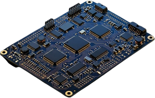
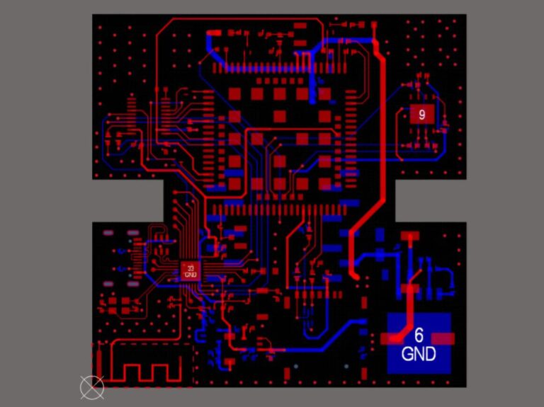
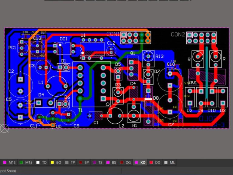
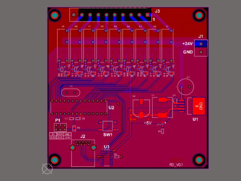
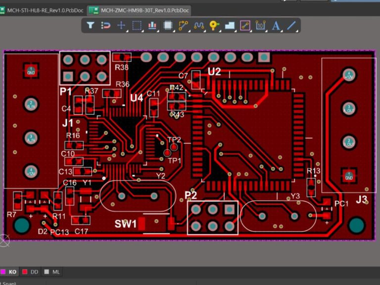
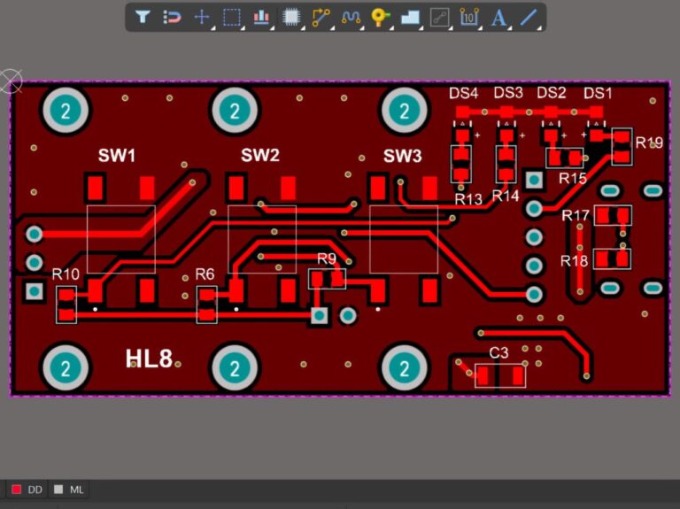
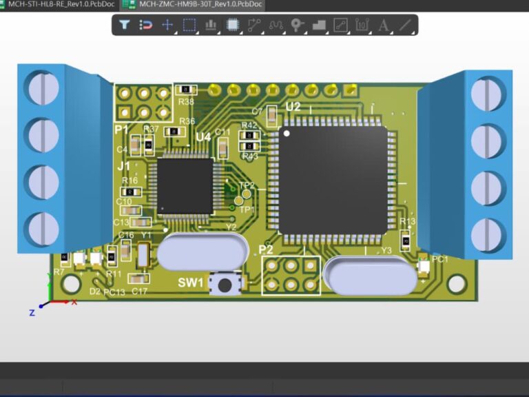
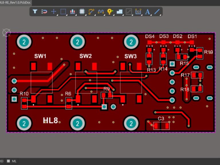
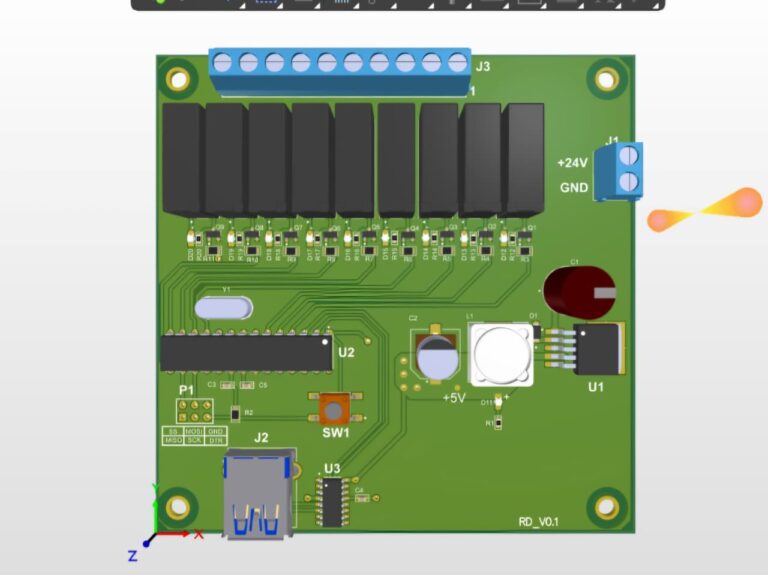
PCB Designs & Hardware We Developed
What We Offer
Multi-Layer PCB Layout Design
High-Quality Layouts from 2 to 12+ Layers
High-Speed Signal Routing
Controlled impedance and signal integrity focused
Schematic Capture & Circuit Design
Accurate schematics using industry-standard tools
EMI / EMC Optimization
Noise reduction and compliance-driven layouts
Component Footprint Creation
Custom footprints and library development
Gerber & Manufacturing Files
Production-ready outputs with all required files
Reverse Engineering Services
Convert existing boards to schematics and layouts
Prototype PCB Development
Quick turnaround for prototypes and pilot builds
DFM & BOM Optimization
Design for manufacturability and cost optimization
Embedded Hardware Integration
Seamless integration with embedded systems
SMT / THT PCB Design
Optimized for both SMT and THT manufacturing
PCB Troubleshooting & Redesign
Debug, analyze and improve existing designs
Have a project or repair requirement?
Let’s build something innovative together.
